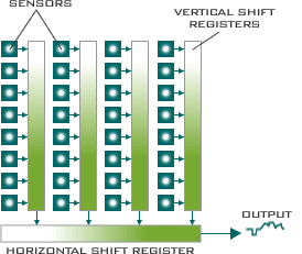
This diagram illustrates the general layout of the most
common type of CCD array, the Interline Transfer CCD. The CCD is composed of
precisely positioned light sensitive semiconductor elements arranged as rows
and columns. Each row in the array represents a single line in the resulting
image. When light falls onto the sensor elements, photons are converted to
electrons, the charge accumulated by each element being proportional to the
light intensity and exposure time. This is known as the integration phase.
After a pre determined period of time the accumulated charge is transferred to
the vertical shift registers.
In cameras conforming to the video standards mentioned
above the charge transfer to the vertical shift registers is accomplished in
two stages. Initially the charge in the odd numbered rows is transferred,
followed by the even rows. Next the charges in the vertical registers are
shifted into the horizontal shift register and clocked to the CCD output.
Consequently all the odd rows are clocked out first (odd field) followed by all
the even rows (even field). The rate at which the charge from the horizontal
shift registers is clocked out is governed by the number of elements (pixels)
per row and the video standard the camera complies with.
An inherent problem associated with the interline
transfer CCD lies in the fact that the vertical shift registers running across
the array are insensitive areas and as such act as blind spots. One way of
overcoming this is to fabricate micro lenses over each element thereby
increasing the effective area of the cell. The lenses also help with the
smaller format CCD. Because of the electrical characteristics of the
semiconductor substrate on which the CCD is formed each cell has an absolute
minimum separation from adjacent cells. Therefore smaller CCDs require smaller
cells. Reducing cell size reduces the amount of accumulated charge, using
lenses increases the incident light.
Another way of overcoming the problem caused by the
vertical shift registers is to do away with them and utilize a different charge
transfer mechanism. Frame Transfer CCDs do exactly that. This type of CCD has a
separate storage area into which the charge is directly transferred from each
cell. This process has to be performed rapidly in order prevent blurring as
transfer occurs during the exposure time. Once in the storage area the charge
can be clocked out in a similar manner to the interline transfer device.


1 comment:
Good content anpr solutions in dubai
Post a Comment